What are the key considerations for routing traces on a rigid flex pcb manufacturers?
key considerations for routing traces on a rigid flex pcb manufacturers
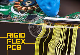
Rigid-flex circuit boards offer significant design flexibility for electronic devices. By combining rigid sections with flexible ones, these innovative technologies enable engineers to optimize space utilization and fit components in tight spaces while also achieving unique form factors. However, it is important to explore the key design guidelines and manufacturing considerations that are associated with rigid-flex PCB technology before utilizing it in an electronic device. This article will explore some of these critical aspects and help you understand how to properly route traces on a rigid flex pcb manufacturers.
Flexibility Analysis: Performing detailed flexibility analysis of rigid flex pcb manufacturer is critical for ensuring that the flexible portions of these circuit boards can withstand repeated bending cycles and maintain structural integrity over their operational lifespan. Detailed flexibility analysis is achieved through the careful selection of materials for both rigid and flexible portions of the board, layer stackup configuration, and application of stiffeners.
Manufacturability Considerations: Integrating manufacturability considerations into the design process for rigid-flex PCBs is essential to facilitating streamlined production processes and minimizing material waste during fabrication. Rigid-flex PCBs require specialized lamination techniques to ensure precise bonding between rigid and flexible sections of the board, which is necessary to preventing delamination during operation.
What are the key considerations for routing traces on a rigid flex pcb manufacturers?
Bend Radius Considerations: Routing traces in compliance with bend radius considerations is crucial for ensuring that mechanical stress on conductive traces is evenly distributed during bending operations and does not exceed acceptable thresholds. In addition, ensuring that copper layers are uniformly switched back and forth between rigid and flexible portions of the board can help to balance force transmission across the flex and rigid areas of the board and eliminate mechanical stresses that may damage them.
Platted Hole Considerations: In general, it is recommended to avoid placing plated holes, vias, and pads in the area of a bending zone. These flex regions can apply mechanical stresses that may tear or harm the structure of plated holes close to them. It is also helpful to keep these plated holes away from the edges of the board, as these are more susceptible to tearing and delamination during flexion.
Dielectric Thickness: Incorporating varying thicknesses of dielectric layers between rigid and flex sections of the PCB can minimize cross-coupling between signals and reduce signal loss. This is particularly effective when paired with proper grounding of the rigid section of the circuit board.
During the routing process, it is also advisable to use dummy traces in flexible areas of the circuit board to decrease areas of high stress, increase the mechanical sturdiness of these traces, and prevent tracing errors. In addition, it is critical to utilize straight, perpendicular traces whenever possible, as curves and turns can cause traces to break or fail during flexing. Lastly, it is important to round off any sharp corners on the traces in flexible areas, as these could be prone to peeling during flexion. Taking these DFM tips into consideration will allow your rigid-flex PCB to deliver superior performance and reliability when compared to traditional rigid or flexible circuit boards.