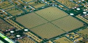
HDI Circuit Boards
A high-density interconnect circuit board (HDI) can improve product performance and reduce the size of a PCB. This makes it an excellent choice for a variety of applications, including mobile / cellular phones, touch-screen devices, laptop computers and digital cameras as well as military tech such as smart munitions or avionics. As such, it’s no surprise that HDI is making a big impact across various industries and markets.
However, with the improved reliability and stability that comes along with these smaller designs, it’s also important to understand the cost implications associated with using hdi circuit board. HDI boards require more layers to make and are often more expensive than standard multilayer PCBs. This is largely due to the increased material and assembly costs involved with a higher layer count, as well as the additional steps required in manufacturing.
The most significant factor that determines the cost of a HDI PCB is the number of sequential laminations. This is because the etching process for HDI PCBs can be a lengthy and complex one, especially for buried via stack-ups.
Cost Implications of Using HDI Circuit Boards
In addition, when deciding on the right HDI stack-up for your design, it’s important to consider the number of holes and their locations. For example, a large hole to copper gap can cause signal crosstalk issues. To mitigate these issues, it’s a good idea to use a smaller hole size or an easy-to-process low-thickness dielectric material for the holes.
Another factor that contributes to the cost of an HDI circuit board is the type and quality of materials used for both the core and surface finishes. The ideal core material for an HDI circuit board is resin-coated copper (RCC), which allows for greater electrical conductivity while lowering the risk of impedance mismatch, signal crosstalk and electromagnetic interference (EMI). The best surface finish for an HDI circuit board is an immersion tin, which provides the highest level of corrosion resistance and solderability.
Other factors that can affect the cost of an HDI circuit board include the layout and component selection. For example, reducing trace widths to increase density can help with manufacturing and design efficiency, but it can also lead to more errors and a higher overall cost. It’s important to discuss your layout with an experienced engineer before you begin the manufacturing process, to ensure that the final product is optimized for manufacturability and cost.
Finally, when designing an HDI circuit board, it’s a good idea to consider the use of via in pad (Via-in-Pad). This process allows you to place a conductive or non-conductive fill into the flat lands on your PCB. This allows you to connect components closer together and can significantly cut down on transmission times as well as crossing delays. It’s a great option for complex ICs, such as BGAs and QFNs, as it eliminates the need for pin outs and simplifies thermal management.